Physical Design & Signoff Engineering

Founded by engineers with decades of hands on semiconductor experience.

Seminovaa is a physical design and signoff partner built for precision from day one. We help chip teams close floorplans, hit timing, and reach clean signoff at the pace advanced nodes demand.

Seminovaa is a specialized semiconductor design services company built around deep Physical Design and signoff expertise: floorplanning, timing closure with full STA signoff, power optimization, DRC, LVS and EM/IR signoff, and pre-silicon DFT at advanced process nodes. We partner with global semiconductor leaders to deliver high performance silicon that is right the first time, from RTL through GDSII.

Enquire now

What We Do

One discipline, held to a signoff standard. A deliberate path to a full ASIC Design House.

We do not spread ourselves across the whole flow. We go deep on Physical Design and signoff, and we build outward from that strength.

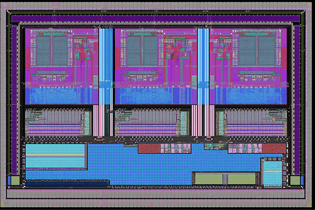
RTL to GDSII physical design
01 / Core

RTL to GDSII & Signoff Closure

Floorplanning, placement, CTS, routing and ECO. Timing closure across corners with full STA signoff. Power optimization. DRC, LVS and EM/IR signoff. Pre-silicon DFT: scan insertion, ATPG and BIST planning, so test coverage is built in, not bolted on at the end.

  • Floorplanning
  • CTS & routing
  • STA signoff
  • DRC / LVS
  • EM/IR
  • Scan & ATPG
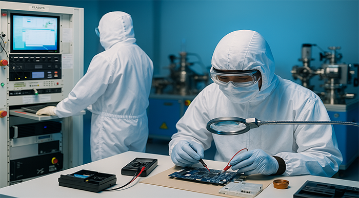
Post-silicon validation lab
02

Test Engineering & Post Silicon Validation

Support for silicon bring up, characterization and validation, from tapeout through production readiness.

  • Silicon bring-up
  • Characterization
  • Validation
Our Scope

We take your design to tapeout ready GDSII. On purpose, we stop there.

We take your design from spec or RTL through to a tapeout ready GDSII: floorplanning, place and route, timing closure with STA signoff, power optimization, pre-silicon DFT, and full signoff across DRC, LVS and EM/IR. Manufacturing, packaging and test remain with you or your foundry partner of choice. That boundary is a choice, not a limitation. It keeps our focus, and our accountability, exactly where chip teams need it most.

Spec / RTLStage 1
Our scope, start to finishSeminovaaPhysical Design & Signoff
Tapeout ready GDSIIStage 3
Manufacturing, packaging & testOutside our scope, by design. With you or your foundry partner.
Our Vision

Engineers who know their tools, including the newest ones.

EDA tools keep getting smarter, and we see that as an advantage for our clients, not a threat to our engineers. We train our Physical Design team to use AI assisted flows for the repetitive, data heavy parts of the job, so more of their time goes into the judgment calls that decide whether a block actually signs off clean. We are building Seminovaa into the ASIC Design House Indian semiconductor teams turn to first, a position we intend to earn through the blocks we actually deliver, not the ones we promise.

physical design servicesFaster exploration

Faster floorplans, more options tried

AI assisted exploration inside our EDA flow lets us try more floorplan and placement options before we commit, instead of settling for the first one that closes.

ASIC physical design companyCleaner closure

Quicker triage on timing and ECOs

Automated report analysis and violation classification help our engineers get to the root cause of a timing or DRC issue faster, so closure cycles get shorter, not shallower.

semiconductor design services companyHuman judgment

Signoff accountability stays with people

Tools accelerate the work. The decision on whether a block is ready to sign off, and the accountability that comes with it, stays with our senior engineers.

How We Work With You

Engagement models shaped around how you like to work.

VLSI physical design services

Dedicated Team

Individual Seminovaa engineers embedded in your team, on site or offshore, integrated into your workflow and reporting into your program, sized up or down as your needs change, on a time and material basis.

semiconductor signoff services

Project-Based

Fixed scope, timeline and cost for one block or a defined set of blocks, RTL/netlist through tapeout ready GDSII, with payment tied to agreed milestones.

STA timing signoff services

Offshore Development Center

A standing Seminovaa team with its own lead, built around your program and dedicated to it long term, functioning as your India engineering site rather than a set of individual placements.

BEYOND THESE

For a full program, we can also talk Turnkey.

Complete ownership of a defined program, from RTL/netlist to tapeout ready GDSII, under one roof. This is structured deal by deal. Tell us what you need, and we will tell you honestly whether we are the right fit today.

Talk to us
Careers · Growth Pathway

Great physical design talent is scarce. So we build it.

Rather than compete on salary alone, we run a structured path that takes engineers from early career to real subsystem ownership.

Step 1

Hire

Engineers early in their career, chosen for strong fundamentals and the ability to learn fast.

Step 2

Train

Structured, hands on training in floorplanning, timing closure and signoff flows, mentored by senior engineers.

Step 3

Expose

Real project exposure alongside our senior team, with growing ownership of blocks and subsystems.

Step 4

Promote

Engineers who show consistent ownership move into senior roles with client facing responsibility.

Always interested in hearing from strong Physical Design engineers.

Get in touch
The Seminovaa team
About Seminovaa

Founded to be a catalyst in the evolving semiconductor landscape.

Seminovaa combines deep technical expertise, a passion for precision, and a commitment to delivering value from day one, principles that have guided the company since it started.

Mission

To deliver transparent, agile, and premium design execution that bridges the global talent gap, and to become the world's most respected company in the semiconductor domain.

Vision

To be the premier Physical Design and signoff partner for complex ASIC and SoC programs, delivering tapeout ready silicon from India to the world.

Leadership

Experienced engineers and domain specialists.

Our leadership brings decades of semiconductor product development, engineering services and industry building.

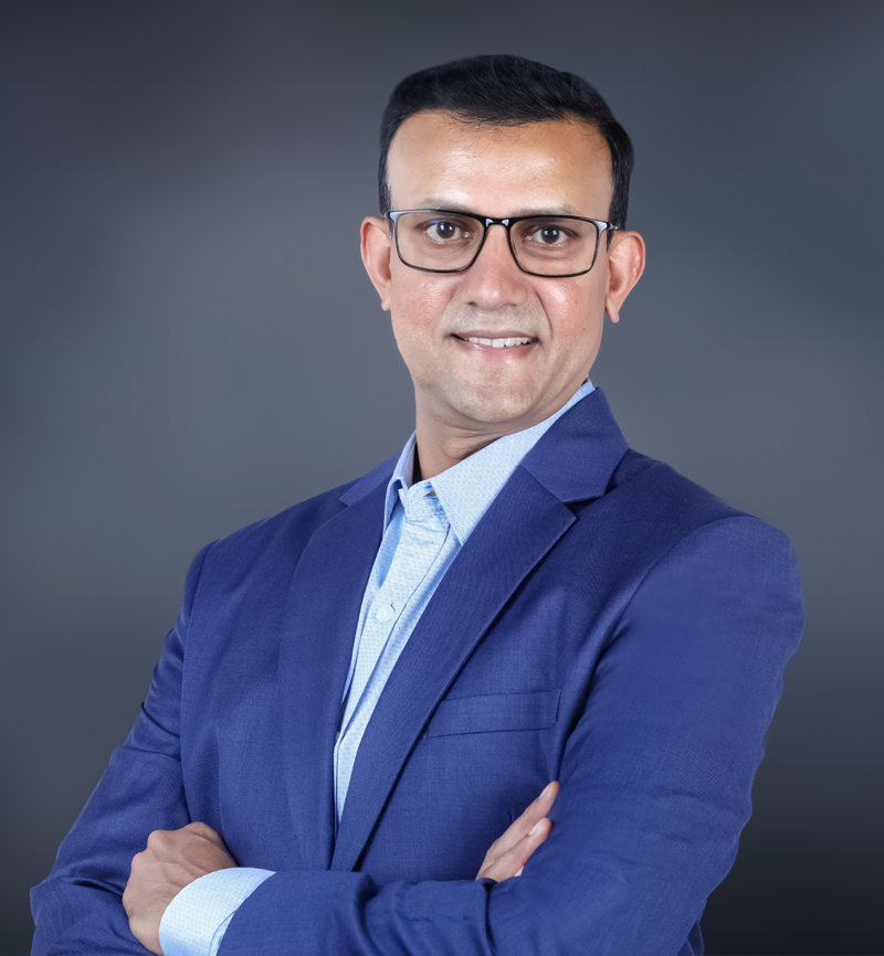
Abutaahir Bhadusha, Founder and CEO
Founder & CEO

Abutaahir Bhadusha

More than 25 years in semiconductor product development, engineering services and business growth, with over 50 semiconductor design projects delivered across mobile, communication, networking and storage. He founded Seminovaa in 2025 to deliver high-value semiconductor design and development from India to the global market.

Read more

He has held key leadership roles at Cadence, Qualcomm, LSI Corporation (USA), RapidBridge (USA), Open-Silicon and Avant! (acquired by Synopsys), expanding engineering capabilities and organizational presence across India and the U.S.

Education: B.E. from Vellore Institute of Technology (VIT) and the PGP program (Executive MBA equivalent) from UCLA.

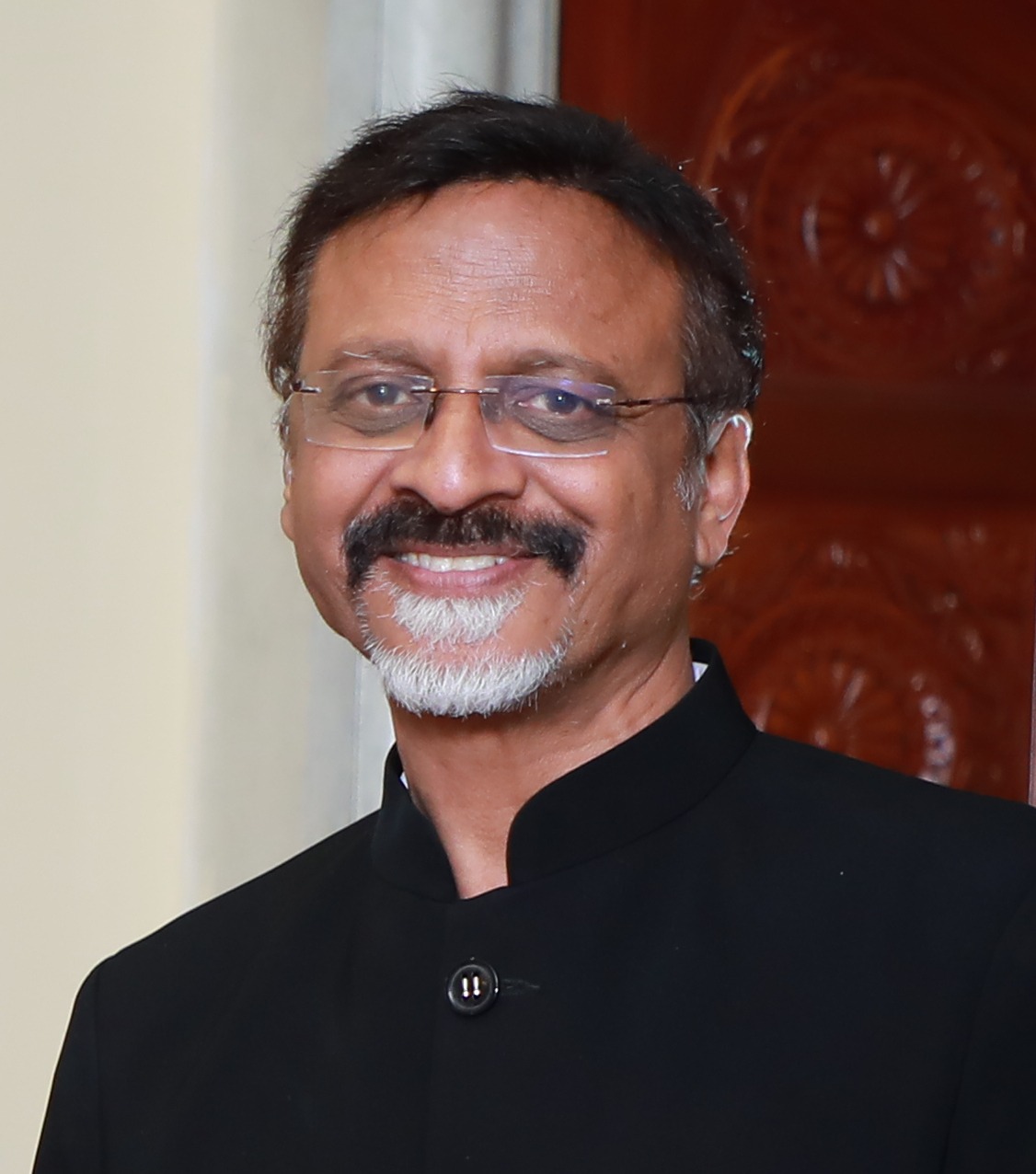
Dr. Satya Gupta, Technical Advisor
Technical Advisor

Dr. Satya Gupta

Part of the worldwide semiconductor and electronics industry for more than 40 years. After 12 years at Intel, he co-founded four companies: Intel Micro-Electronics, Open-Silicon, Concept-2-Silicon and SenZopt. He is currently president of the VLSI Society of India.

Read more

Founding member of the India Semiconductor Association (IESA) in 2005 and its chairman in 2012-13 and 2020-21. He also co-founded and served as CEO of the EPIC Foundation, a non-profit for developing Indian electronics products.

His mission is to make India an electronics and semiconductor product nation, taking VLSI design education to 500+ colleges and establishing "1-TOPS: One Chip Tape-Out Per Student" before graduation.

Recognition includes the IEEE Gordon Bell award for the fastest supercomputer, Best Private Semiconductor Company (Open-Silicon, Global Semiconductor Alliance), the Distinguished Alumni Award from BITS Pilani, and Lifetime Achievement Awards from the VLSI Society of India, DVCON and Mentor Graphics.

He is visiting faculty at IIT Roorkee, IIT Gandhinagar and Gati Shakti University, and sits on the Board of Governors at BMS-ITM, Bangalore.

Get in touch

Let's talk about your next tapeout.

Whether it is a defined work package, a team extension, or an early conversation about where Seminovaa can help, we would like to hear from you.

Get in touch
JP Classic, Ground Floor, 157/1
Corporate Block 1, Phase 2, EPIP
Zone, Whitefield, Bangalore-560066
Karnataka
Need support?
General & Sales
info@seminovaa.com
sales@seminovaa.com
Careers
careers@seminovaa.com
↑