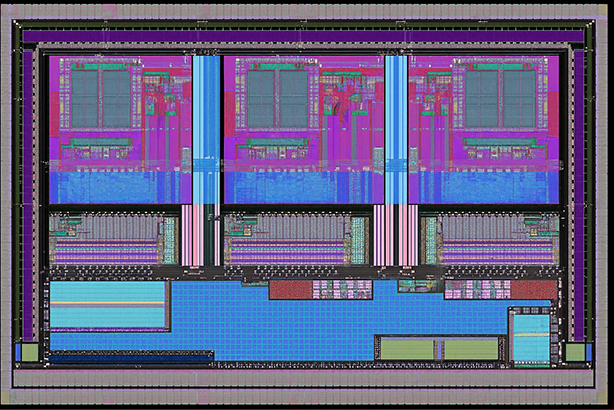
SoC/ASIC Design & Verification

At Seminovaa™, we design and verify high-performance ASICs and complex SoCs tailored to your specific application needs. Our engineering teams bring deep domain expertise across the entire chip development cycle — from RTL design, IP integration, and low-power architecture to functional verification using industry-standard methodologies like UVM.

global-semiconductor-design-team
Our Expertise Covers
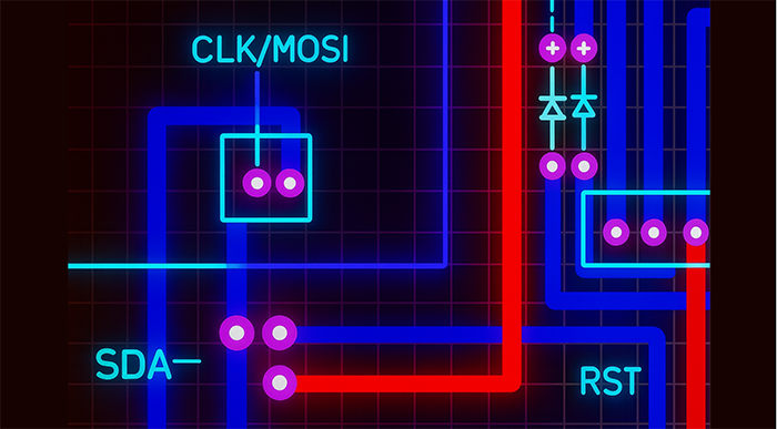
  • TL design & IP integration
  • Low-power architecture & multi-voltage design
  • Testbench creation (C, SystemVerilog, UVM)
  • Protocol verification (PCIe, DDR, Ethernet, AMBA)
  • Debugging with waveform, logs, TARMAC, and co-simulation
Ensuring First-Pass Silicon Success

We employ a rigorous verification strategy — including simulation, formal verification, and emulation — to identify and address design issues early, reducing risk and accelerating time-to-market

AI-Enhanced Verification

To maximize efficiency and coverage, Seminovaa integrates Gen-AI/Agentic-AI into its DV workflows:

Smart test generation: AI models create optimized, high-coverage test scenarios.

Automated bug triage: AI assists in root-cause analysis for faster debug cycles.

Coverage gap prediction: ML identifies untested design areas before closure.

Regression optimization: AI prioritizes critical test cases to shorten run times.

The Result: Comprehensive verification coverage, reduced debug cycles, and a higher probability of on-time, first-pass silicon delivery.

Enquire Now

RTL To GDS II (Physical Design), DFT (Pre-Silicon) and Signoff Closure

global-semiconductor-design-team

At Seminovaa™, we deliver comprehensive Physical Design services — from RTL to GDSII — integrated with Design-for-Test (DFT) and Static Timing Analysis (STA) to ensure your design is functional, testable, timing-accurate, and tape-out ready.

Our Expertise Covers

  • Synthesis, floorplanning, placement & routing
  • Clock Tree Synthesis (CTS) and power planning
  • DFT insertion, scan chain stitching, and ATPG generation
  • Physical verification (DRC/LVS), sign-off, and layout finishing
Precision in Timing & Quality

We apply advanced STA to validate timing across multiple corners, modes, and scenarios — ensuring setup, hold, skew, and latency targets are consistently met under PVT variations.

AI-Driven Optimization

To push the boundaries further, Seminovaa integrates Gen-AI/Agentic-AI models into every stage of implementation:

Intelligent floorplanning: dynamic placement optimization for PPA (Performance, Power, Area) goals.

Automated timing closure: real-time ECO, re-buffering, and cell swap suggestions.

Smart power optimization: early detection of redundant switching and suboptimal clock gating.

Predictive DRC/LVS analysis: ML-trained anomaly detection to preempt violations before sign-off.

The Result: Faster iterations, higher design quality, and increased probability of first-pass silicon success.

Enquire Now

Test Engineering/Post-Silicon Validation

At Seminovaa™, we bridge the gap between silicon and system with robust post-silicon validation and test engineering services. Our goal is first-time-right silicon, achieved through comprehensive bring-up, validation, and characterization.

Our Expertise Covers
  • DFT & ATPG Support
  • Production test strategy and ATE program development
  • Silicon bring-up and functional validation
  • Failure Analysis Support
  • Electrical characterization across PVT corners
  • High-speed interface validation (PCIe, DDR, Ethernet, etc.)
  • Corner testing and stress validation
  • Yield analysis and optimization
 post-silicon-validation-lab-testing
Driving Silicon Quality & Reliability

We ensure every chip meets performance and reliability targets through system-level validation, failure analysis, and root-cause debugging.

Enquire Now

Custom Layout Design (Analog/Mixed Signal)

At Seminovaa™, we bring deep expertise in Custom Layout Design for analog, mixed-signal, RF, and high-performance circuits. Our strength lies in combining precision craftsmanship with EDA-driven automation to deliver layouts that are optimized for performance, power, area (PPA), reliability, and manufacturability. We focus on Enabling Semiconductor companies to accelerate time-to-market while ensuring first-silicon success.

 post-silicon-validation-lab-testing
Our Expertise Covers
  • Full-Custom Transistor-Level Layout for analog, mixed-signal, and high-speed blocks.
  • Proven techniques in device matching, symmetry, common centroid, shielding, and guard-ring structures.
  • Hands-on execution across amplifiers, comparators, PLLs, ADC/DACs, SERDES, and PHYs.
  • Layout practices that ensure robust sign-off, scalability, and first-pass silicon success.

We'd love to hear from you.

Whether you’re exploring Seminovaa’s semiconductor services, seeking technical expertise, or looking for ways to elevate your product with our deep-tech solutions — we’re here to help.

Our team is ready to understand your needs, share insights, and create solutions that deliver real impact.

Scroll